HANA Micron Logo
전체메뉴
Main visual.

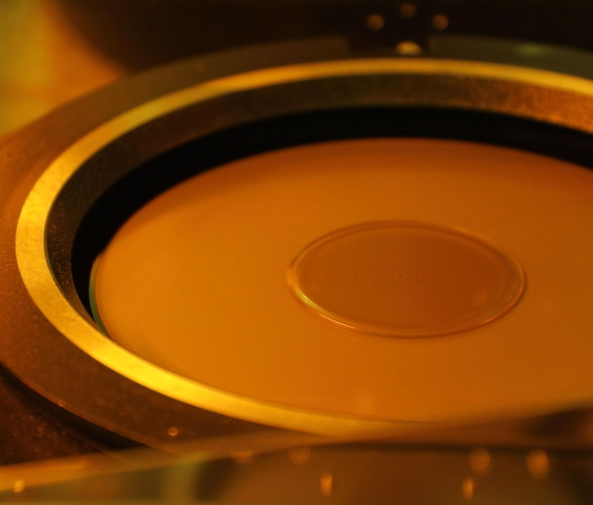
Bump
We offer solder bumping, Cu bumping solutions
for WLCSP and flip-chip.
- WLCSP(8inch/12inch)
- High Performance RDL
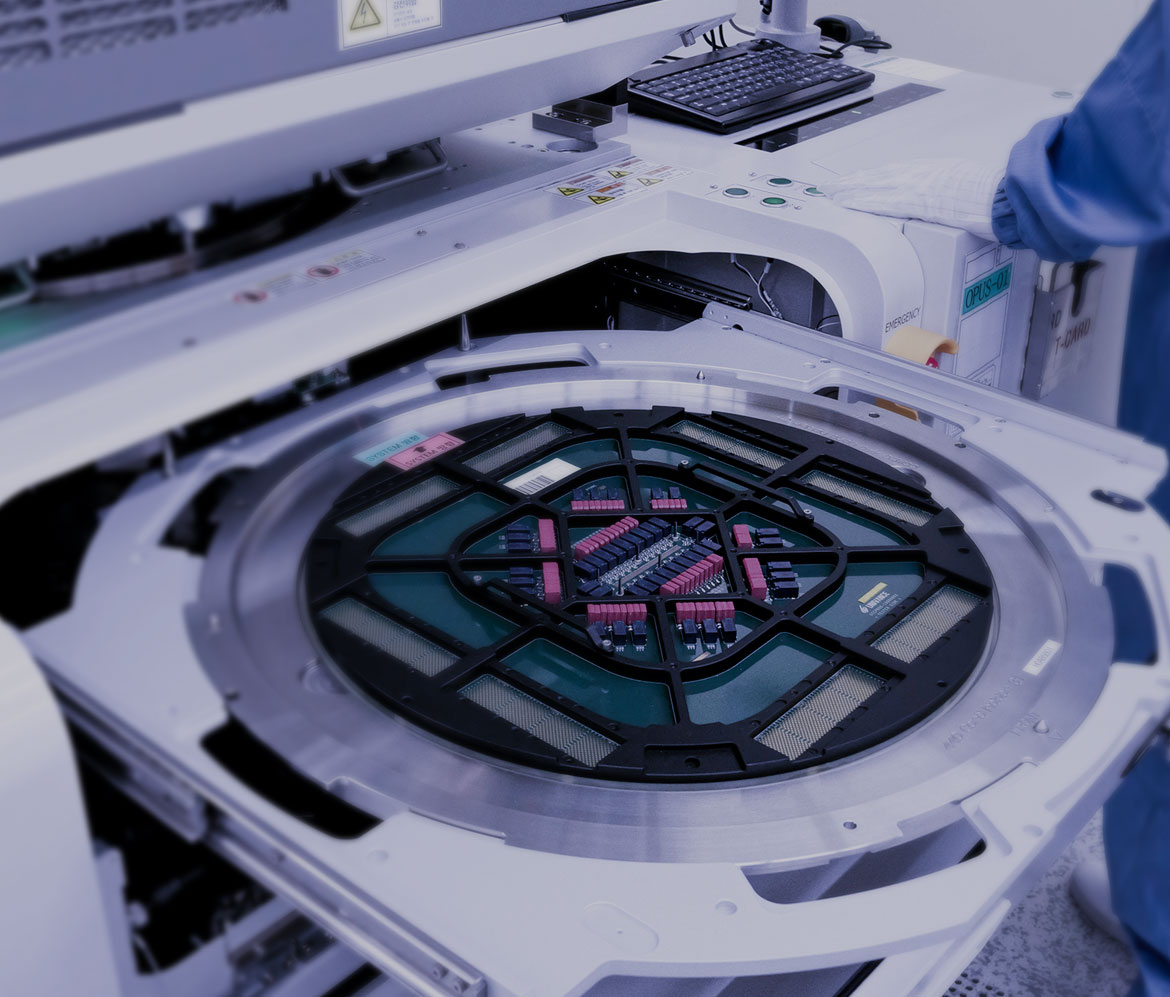
Test
We provide test solutions for the electrical test
of wafer level chips (IC) with molded bumps.
- Wafer Probe Test
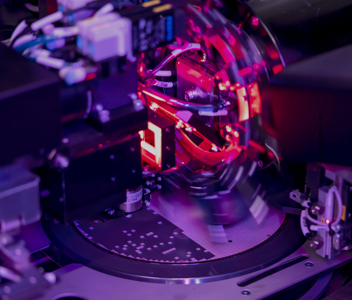
DPS
We provide DSP (Die Processing Service) such as Back grinding, Sawing, Laser Marking, Tape & Reel to the electrically tested product.
- Advanced Technology
BUSINESS
We generate a new value for the semiconductor
product through continuous technological innovation.
Semiconductor Package and Test Total Solution Provider
INFORMATION
HANA WLS makes dreams come true in the global arena.
-
Total Solution
We are a WLP full turnkey solution provider.
-
Advanced Technology
We are a WLP
full turnkey solution provider. -
Value Preposition
We offer unique and
differentiated technologies. -
HANA Micron Group
We discover and suggest the optimal
solution that fits customers’ needs.